A solder pad is the part of a printed circuit board — or PCB — that supports the pins of components like transistors and chips. Typically, when devices break or components are removed from PCBs, it can result in damaged and missing solder pads.
The following instructional steps will help you repair a missing solder pad, so your PCB is ready for new components and further use. This entire process, including the cutting of traces from the circuit frame library that are to be joined to the traces on the existing PCB.
Steps to Fix a Missing Solder Pad
Before beginning the repair process, you’ll want to gather the following materials:
- C-clamps
- Isopropyl alcohol and wipes
- Lint-free cloth
- Magnifying glass or microscope
- Solder and soldering iron
- Flux
- Circuit frame
- Epoxy resin and hardener
- Toothpicks
- ESD safe Kapton tape
- X-Acto knife
- Safe ESD cutting surface
Once you’ve collected all of the required materials, carefully follow these 10 steps to complete the PCB repair process:
- Cleaning the damaged pad: Thoroughly clean the damaged area with isopropyl alcohol, and follow up by drying the area with a lint-free cloth or compressed/canned air.
- Removing the damaged pad: Use an X-Acto knife to carefully cut away the damaged pad.
- Cleaning the area around/under the damaged pad: After removing the pad, clean the area immediately around/under the pad. Be sure to thoroughly remove any damaged or burned laminate from the area.
- Removing the solder mask: Using a toothpick, remove any existing solder mask from the conductor.
- Repeat cleaning the area: Using isopropyl alcohol, conduct another thorough cleaning of the area. Follow up by drying the area with a lint free cloth or compressed/canned air.
- Tinning the conductor: Select the appropriate solder alloy to tin the conductor area where the conductor will be attached.
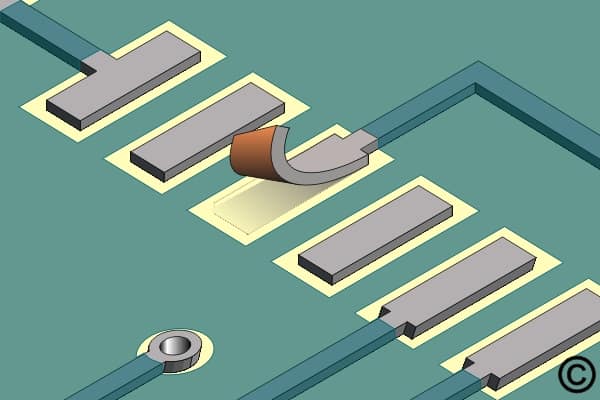
- Selecting the appropriate circuit frame: Using an X-Acto knife, cut out a new conductor from the appropriate circuit frame.
- Tinning the new pad/conductor: With the appropriate solder alloy, tin the pad/conductor area that will overlap the original trace. Now, mix up a small amount of epoxy resin and hardener, and apply it to the area on the PCB. You can either use open air to cure it, or you can use an oven — but be sure to follow all manufacturer guidelines.
- Soldering the new pad/trace to the conductor: Use Kapton tape to place and hold the replacement pad. Use the appropriate solder alloy to make a lap joint.
- Clamping and curing: Clamp the new pad/trace in place and cure. Once cured, remove the clamp and clean the pad/trace with isopropyl alcohol. Note: This is a good time to run a quick electrical continuity test. Once everything checks out, you may also want to envelop the edges of the new pad/trace with epoxy or solder mask to give the area increased mechanical strength.